Turn-On Methods of A Thyristor

A thyristor can be switched from a nonconducting state to a conducting state in several ways described as follows.
1.9.1 Forward Voltage Triggering
When anode-to-cathode forward voltage is increased with gate circuit open, the reverse biased junction J2 will have an avalanche breakdown at a voltage called forward breakover voltage VBO. At this voltage, a thyristor changes from OFF state (high voltage with low leakage current) to ON-state characterised by a low voltage across it with large forward current. The forward voltage-drop across the SCR during the ON state is of the order of 1 to 1.5 V and increases slightly with load current.
1.9.2 Thermal Triggering (Temperature Triggering)
Like any other semiconductor, the width of the depletion layer of a thyristor decreases on increasing the junction temperature. Thus, in a thyristor when the voltage applied between the anode and cathode is very near to its breakdown voltage, the device can be triggered by increasing its junction temperature. By increasing the temperature to a certain value (within the specified-limits), a situation comes when the reverse biased junction collapses making the device conduct. This method of triggering the device by heating is known as the thermal triggering process.
1.9.3 Radiation Triggering (Light Triggering)
In this method, as the name suggests, the energy is imparted by radiation. Thyristor is bombarded by energy particles such as neutrons or photons. With the help of this external energy, electron-hole pairs are generated in the device, thus increasing the number of charge carriers. This leads to instantaneous flow of current within the device and the triggering of the device. For radiation triggering to occur, the device must have high value of rate of change of voltage (dv/dt). Light activated silicon controlled rectifier (LASCR) and light activated silicon controlled switch (LASCS) are the examples of this type of triggering.
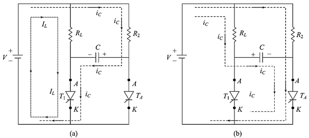
1.9.4 dv/dt Triggering
We know that with forward voltage across the anode and cathode of a device, the junctions J1 and J3 are forward biased, whereas the junction J2 becomes reverse biased. This reverse biased junction J2 has the characteristics of a capacitor due to charges existing across the junction. If a forward voltage is suddenly applied, a charging current will flow tending to turn the device ON. If the voltage impressed across the device is denoted by V, the charge by Q and the capacitance by Cj, then
$latex \displaystyle {{i}_{c}}=\frac{{dQ}}{{dt}}=\frac{d}{{dt}}{{C}_{j}}V={{C}_{j}}\frac{{dV}}{{dt}}+V\frac{{d{{c}_{j}}}}{{dt}}$
The rate of change of junction capacitance may be negligible as the junction capacitance is almost constant. The contribution to charging current by the later term is negligible. Hence, the above Equation reduces to
$latex \displaystyle {{i}_{c}}={{C}_{j}}\frac{{dV}}{{dt}}$
Therefore, if the rate of change of voltage across the device is large, the device may turn-on even though the voltage appearing across the device is small.
1.9.5 Gate Triggering
This is the most commonly used method for triggering SCRs. In laboratories, almost all the SCR devices are triggered by this process. By applying a positive signal at the gate terminal of the device, it can be triggered much before the specified breakover voltage. The conduction period of the SCR can be controlled by varying the gate signal within the specified values of the maximum and minimum gate currents. For gate triggering, a signal is applied between the gate and the cathode of the device. Three types of signals can be used for this purpose. They are either d.c. signals, pulse signals or ac signals.
D.C. Gate Triggering: In this type of triggering, a d.c. voltage of proper magnitude and polarity is applied between the gate and the cathode of the device in such a way that the gate becomes positive with respect to the cathode. When the applied voltage is sufficient to produce the required gate current, the device starts conducting. One drawback of this scheme is that both the power and control circuits are d.c. and there is no isolation between the two. Another disadvantage of this process is that a continuous d.c. signal has to be applied, at the gate causing more gate power loss.
A.C. Gate Triggering: A.C. source is most commonly used for the gate signal in all application of thyristor control adopted for a.c. applications. This scheme provides the proper isolation between the power and the control circuits. The firing angle control is obtained very conveniently by changing the phase angle of the control signal. However, the gate drive is maintained for one half cycle after the device is turned ON, and a reverse voltage is applied between the gate and the cathode during the negative half cycle. The drawback of this scheme is that a separate transformer is required to step down the a.c. supply, which adds to the cost.
Pulse Gate Triggering: This is the most popular method for triggering the device. In this method, the gate drive consists of a single pulse appearing periodically or a sequence of high frequency pulses. This is known as carrier frequency gating. A pulse transformer is used for isolation. The main advantage of this method is that there is no need of applying continuous signals and hence, the gate losses are very much reduced. Electrical isolation is also provided between the main device supply and its gating signals.


latest video

news via inbox
Nulla turp dis cursus. Integer liberos euismod pretium faucibua