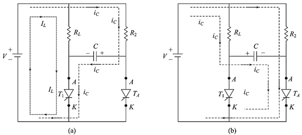
Static (VI) Characteristics of SCR
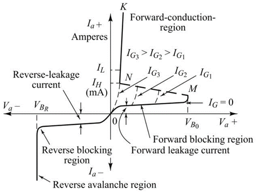
An elementary circuit diagram for obtaining static V-I characteristics of a thyristor is shown in Figure 17. Here, the anode and cathode are connected to the main source through a load. The gate and cathode are fed from another source Eg. The static V-I characteristic of an SCR is shown in Figure 18. Here, Va is the anode-cathode voltage and Ia is the anode current. The thyristor V-I characteristics is divided into three regions of operation.
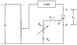
Figure 17
Reverse Blocking Region: When the cathode is made positive with respect to anode with the switch, s open, the thyristor becomes reverse biased. In Figure 18, OP is the reverse blocking region. In this region, the thyristor exhibits a blocking characteristic similar to that of a diode. In this reverse biased condition, the outer junction J1 and J3 are reverse biased and the middle junction J2 is forward biased. Therefore, only a small leakage current (in mA) flows. If the reverse voltage is increased, then at a critical breakdown level called reverse breakdown voltage VBR, an avalanche will occur at J1 and J3 increasing the current sharply. If this current is not limited to a safe value, power dissipation will increase to a dangerous level that may destroy the device. Region PQ is the reverseavalanche region. If the reverse voltage applied across the device is below this critical value, the device will behave as a high-impedance device (i.e., essentially open) in the reverse direction.
The inner two regions of the SCR are lightly doped compared to the outer layers. Hence, the thickness of the J2 depletion layer during the forward biased conditions will be greater than the total thickness of the two depletion layers at J1 and J3 when the device is reverse biased. Therefore, the forward breakover voltage VBO is generally higher than the reverse break-over voltage VBR.
Forward Blocking Region: In this region, the anode is made positive with respect to the cathode and therefore, junctions J1 and J3 are forward biased while the junction J2 remains reverse biased. Hence, the anode current is a small forward leakage current. The region OM of the V-I characteristic is known as the forward blocking region when the device does not conduct.
Forward Conduction Region: When the anode to cathode forward voltage is increased with the gate circuit kept open, avalanche breakdown occurs at the junction J2 at a critical forward break-over voltage (VBO), and the SCR switches into a low impedance condition (high conduction mode). In Figure 18, the forward breakover voltage is corresponding to the point M, when the device latches on to the conducting state. The region MN of the characteristic shows that as soon as the device latches on to its ON state, the voltage across the device drops from say, several hundred volt to 1-2 volt, depending on the rating of the SCR, and suddenly a very large amount of current starts flowing through the device. The part NK of the characteristic is called as the forward conduction state. In this high conduction mode, the anode current is determined essentially by the external load impedance. Therefore when the thyristor conducts forward current, it can be regarded as a closed switch.
Figure 18
VB0 = Forward breakover voltage; VBR = Reverse breakover voltage;
IG = Gate current; IL = Latching current; IH = Holding current
When a gate-signal is applied, the thyristor turns-on before VBO is reached. The forward voltage at which the device switches to ON state depends upon the magnitude of gate current; higher the gate current, lower is the forward breakover voltage. Figure shows that for gate current IG = 0, the forward breakover voltage is VBO. For IG1, the forward breakover voltage is less than VBO and for IG2>IG1, it is still further reduced. In practice, the magnitude of gate-current is more than the minimum gate current required to turn-on the SCR. The typical gate current magnitudes are of the order of 20 to 200 mA.
Once the SCR is conducting a forward current that is greater than the minimum value, called the latching current (IL), the gate signal is no longer required to maintain the device in its ON state. Removal of the gate current does not affect the conduction of the anode current. The SCR will return to its original forward blocking state if the anode current falls below a low level, called the holding current (IH). For most industrial applications, this holding current (typically 10 mA) can be regarded as being essentially zero. Note that latching current is associated with turn-on process and holding current with turn-off process. The holding current is usually lower than, but very close to the latching current. Hence, from the above discussion it becomes clear that the more convenient, reliable and efficient method of turning on the device employs the gate drive.


latest video

news via inbox
Nulla turp dis cursus. Integer liberos euismod pretium faucibua