Gate Turn-Off Thyristor
As we know that once an SCR is turned ON by the gate signal, the gate loses control and it can be brought back to the blocking state only by reducing the forward current to a level below that of the holding current. This is the serious deficiency in thyristors that prevent their use in switch mode applications. This section describes the structure and operation of thyristors that have a gate turn-off capability, the so-called gate turn-off thyristors or GTOs.
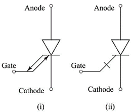
The gate turn-off thyristor (GTO) incorporates many of the advantages of the conventional thyristor and the high-voltage switching transistor. It is a PNPN device that can be triggered into conduction by a small positive gate-current pulse, but also has the capability of being turned-off by a negative gate-current pulse. However, the turn-off current gain is low (typically 4 or 5). For example, a 4000V, 3000A device may need –750 A gate current to turn it OFF. This facility allows the construction of inverter circuits without the bulky and expensive forced commutating components associated with conventional thyristor circuitry. The GTO is a three-terminal device with anode, cathode and gate terminals. The various circuit symbols are shown in Figure 15. The two-way arrow convention (Figure 15(i)) on the gate lead distinguishes the GTO from the conventional thyristor.
Figure 15
Figure 16 shows the two-transistor analogy of the GTO. Like the conventional thyristor, the GTO switches regeneratively into the onstate when a positive gating signal is applied to the base of the N-P-N transistor. In a regular thyristor, the current gains of the N-P-N and P-N-P transistors are large in order to maximize gate sensitivity at turn-on and to minimize on-state voltage drop. But this pronounced regenerative latching effect means that the thyristor cannot be turned-off at the gate.
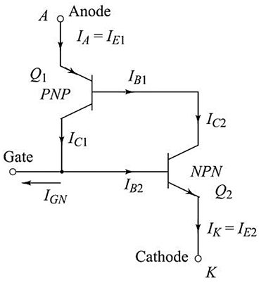
Figure 16
Internal regeneration is reduced in the GTO by a reduction in the current gain of the P-N-P transistor, and turn-off is achieved by drawing sufficient current from the gate. The turn-off action may be explained as follows. When a negative bias is applied at the gate, excess carriers are drawn from the base region of the N-P-N transistor, and the collector current of the P-N-P transistor is diverted into the external gate circuit. Thus, the base drive of the N-P-N transistor is removed and this, in turn, removes the base drive of the P-N-P transistor, and stops conduction.


latest video

news via inbox
Nulla turp dis cursus. Integer liberos euismod pretium faucibua