Power Bipolar Junction Transistor
Power BJT Operation and VI Characteristics
Power transistors are devices that have controlled turn-on and turn-off characteristics. These devices are used as a switching device and are operated in the saturation region resulting in low on-state voltage drop. They are turned on when a current signal is given to the base or control terminal. The transistor remains on so long as the control signal is present. The switching speed of modern transistors is much higher than that of Thyristors and are used extensively in dc-dc and dc-ac converters. However, their voltage and current ratings are lower than those of thyristors and are therefore used in low to medium power applications.
The need for a large blocking voltage in the off state and a high current carrying capability in the on state means that a power BJT must have substantially different structure than its small signal equivalent. The modified structure leads to significant differences in the I-V characteristics and switching behavior between power transistors and their logic level counterpart.
A bipolar transistor is formed by adding a second p- or n-region to a pn junction diode. With two n-regions and one p-region, two junctions are formed, and it is known as npn transistor, as shown in Figure 2. With two p-regions and one n-region, it is called as pnp transistor, as shown in Figure 2. The three terminals are named collector, emitter, and base. A bipolar transistor has two junctions, collector-base junction (CBJ) and base-emitter junction (BEJ).

Figure 2
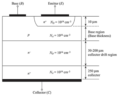
A power transistor is a vertically oriented four-layer structure of alternating p-type and n-type as shown in Figure 3. This is maximizing the cross-section area results in current rating of BJT, minimize the on-state resistance, and thus reduce the power losses. The doping of emitter layer and collector layer is quite large. A special layer called the collector drift region (n-) has a light doping. The thickness of the drift region determines the breakdown voltage of the transistor.
Figure 3
The base thickness is made as small as possible to have good amplification capabilities, however if the base thickness is small the breakdown voltage capability of the transistor is compromised.
Although there are three possible configurations – common base, common emitter, and common collector – the common emitter configuration, which is shown in Figure 4 for a npn transistor, is generally used in switching applications.
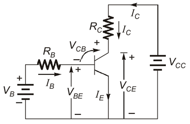
Figure 4
The power transistor has steady state characteristics almost like signal level transistors except that the V-I characteristics has a region of quasi saturation as shown by Figure 5.
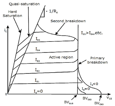
Figure 5
Three regions of operation for a BJT can be recognized:
Cutoff Region: When the base current (IB) is zero, the collector current (IC) is insignificant and the transistor is driven into the cutoff region. The transistor is now in the OFF state. The collector – base and base – emitter junctions are reverse biased in the cutoff region or OFF state, and the transistor behaves as an open switch. In this region: IC = 0 and the collector-emitter voltage VCE is equal to the supply voltage VCC.
Saturation Region: When the base current is sufficient to drive the transistor into saturation. During saturation, both junctions are forward-biased, and the transistor acts like a closed switch. In the quasi saturation and hard saturation, the base drive is applied, and transistor is said to be on. In this region: IC = VCC /RC and VCE = zero
Active Region: In the active region, the collector–base junction is reversed-biased, and the base-emitter junction is forward-biased. The active region of the transistor is mainly used for amplifier applications and should be avoided for switching operation.
The power BJT is never operated in the active region (i.e., as an amplifier) it is always operated between cut-off and saturation.


latest video

news via inbox
Nulla turp dis cursus. Integer liberos euismod pretium faucibua