Basic Operation of SCR
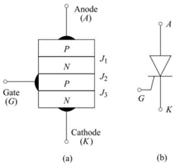
The structure and symbol of the thyristor (SCR) are shown in Figure. It is a four layered PNPN switching device, having three junctions J1, J2 and J3. It has three external terminals, namely, the anode (A), cathode (K) and gate (G). The anode and cathode are connected to the main power circuit. The gate terminal carries a low level gate current in the direction gate to cathode. Normally, the gate terminal is provided at the P layer near the cathode. This is known as cathode gate.
When the end P layer is made positive with respect to the end N layer , the two outer junctions, J1 and J3 are forward biased but the middle junction J2 becomes reverse biased. Thus the junction J2 because of the presence of depletion layer, does not allow any current to flow through the device. Only leakage current, negligibly small in magnitude, flows through the device due to the drift of the mobile charges. This current is insufficient to make the device conduct. The depletion layer, mostly of immobile charges do not constitute any flow of current. In other words, the SCR under the forward biased condition does not conduct. This is called as the forward blocking state or off-state of the device.
When the end n layer is made positive with respect to end p layer, the middle junction J2 becomes forward biased, whereas the two outer junctions, J1 and J3 become reverse biased. The junctions J1 and J3 do not allow any current to flow through the device. Only a very small amount of leakage current may flow because of the drift of the charges. The leakage current is again insufficient to make the device conduct. This is known as the reverse blocking state or off-state of the device.
The width of the depletion layer at the junction J2 decreases with the increase in anode to cathode voltage (since the width is inversely proportional to voltage). If the voltage between the anode and cathode is kept on increasing, a stage comes (corresponding to forward break-over voltage) when the depletion layer at J2 vanishes. The reverse biased junction J2 will breakdown due to the large voltage gradient across its depletion layer. This phenomenon is known as the Avalanche breakdown. Since the other junctions, J1 and J3 are already forward biased, there will be a free carrier movement across all the three junctions resulting in a large amount of current flowing through the device from anode to cathode. Due to the flow of this forward current, the device starts conducting and it is then said to be in the conducting state or on state.


latest video

news via inbox
Nulla turp dis cursus. Integer liberos euismod pretium faucibua