Switching Characteristics of Power MOSFET
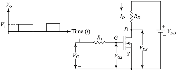
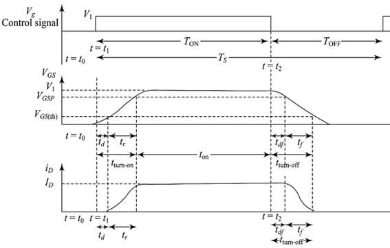
Figure 12(a) shows a steady state switching circuit of a power MOSFET. When a pulse input voltage is applied to the gate of power MOSFET, the device will be turn-on if the gate to source voltage VGS is greater than threshold voltage VGS(th). The switching waveforms of a power MOSFET are illustrated in Figure 12.
At time t = t0, input voltage at the gate of power MOSFET is Vg = 0 and the gate to source voltage VGS is less than threshold voltage VGS(th). At that moment, the device operates in OFF state and the drain current ID is equal to zero and the output voltage is VO = VDS = VDD.
At time t = t1, voltage starts to increase from 0 to V1 and the input capacitance Cgs starts to charge as depicted in Figure. During the turn on delay time td, the capacitance Cgs is charged to gate threshold voltage VGS(th). During rise time tr, the gate to source voltage VGS increases from gate threshold level VGS(th) to the full gate voltage, VGSP to operate the transistor in linear region. In time tr, the drain current increases from 0 to ID. The total turn on time of MOSFET is sum of delay time and rise time.
- Delay time td The delay time td is the time required to charge the input capacitance from its initial value to gate threshold voltage VGS(th).
- Rise time tr The rise time tr is the time required to charge the input capacitance Cgs from gate threshold level VGS(th) to the full gate voltage, VGSP.
- Turn-on time tturn-on The turn-on time is the sum of the delay time td and the rise time tr and it can be expressed as tturn-on = td + tr.
In the turn-off process, the gate voltage Vg is removed t = t2, the input capacitance starts to discharge from gate voltage V1 to VGSP. VGS must be decreased significantly so that VDS starts to increase. The fall time is the time during which input capacitance discharged from VGSP to gate threshold voltage VGS(th). In this time, the drain current decreases from ID to zero. When VGS<VGS(th), the device completely turn off.
The turn-off delay time tdf is the time during which the input capacitance discharges from gate voltage V1 to VGSP.
The fall time tf is the time in which the input capacitance discharges from gate voltage VGSP to VGS(th) and the drain current becomes zero.
The turn-off time is the sum of the turn-off delay time (tdf) and fall time (tf) and it can be represented by tturn-off = tdf + tf.


Figure 12
latest video
news via inbox
Nulla turp dis cursus. Integer liberos euismod pretium faucibua


