Snubber Circuit
Snubber Circuit
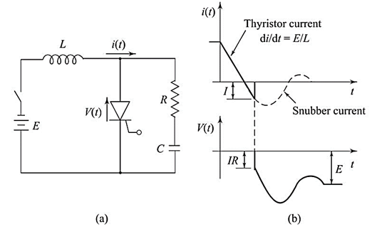
In most power electronic circuits, protection is necessary against the effects of excessive rate of rise of forward voltage (dv/dt) across the devices, which can otherwise cause unintended breakover, leading to a malfunction of the circuit and possible to failure of the devices. The tendency to excessive dv/dt may arise from external causes such as the closing of main supply contactor, or from the operation of the circuit itself. dv/dt suppression is achieved by means of snubber circuit. The snubber circuit basically consists of a series-connected resistor and capacitor placed in shunt with an SCR, as shown in Figure 34. A capacitor C across the thyristor means that any high dv/dt appearing at the thyristor terminals will set up an appropriate current (C dv/dt) in the capacitor. The inductance in the circuit will severely limit the magnitude of the current to the capacitor and hence limit dv/dt. In Figure 34(a), the inductance, L, is the effective circuit inductance and its presence limits the initial di/dt of the device at turn-on. A series inductor, either linear or saturable, may be introduced to augment the supply circuit inductance. Normally, the LCR circuit is slightly underdamped, and when a forward voltage step is applied to it, the peak voltage appearing across the device and its rate of change are both limited to acceptable values. Snubber losses can be appreciable, particularly at high-switching frequencies.
When the thyristor turn-off, there is a brief pulse of reverse recovery current that rises to a peak value, at which time the device blocks. In the absence of an RC snubber, the abrupt interruption of the reverse recovery current in the series inductance, L, will cause transient L di/dt overvoltages that may destroy the device itself or other semiconductors in the converter circuit. If an RC snubber is connected across the thyristor, the reverse recovery current can transfer to the RC path when the device blocks, as shown in Figure 34(b). The voltage across the RC path appears as an oscillatory reverse voltage across the semiconductor. A correctly designed snubber will limit the amplitude of this reverse-recovery voltage and will also limit its rate of rise. By delaying the build-up of reverse voltage across the semiconductor, the recovery losses in the device are also reduced. If the snubber resistance is too small, excessive ringing will occur in the LCR circuit, and the reverse blocking voltage capability of the semiconductor may be exceeded.
Figure 34
When thyristor T1 in Figure 34(a) turns-on, the snubber capacitor, C, discharges into the thyristor, but resistor R limits the discharge current and prevents excessive di/dt at turn-on. However, at turn-off, a forward IR voltage drop suddenly appears across the thyristor due to reverse recovery of the diode, as indicated in Figure 34(b). Thus, the presence of the resistor impairs the forward dv/dt limiting performance of the snubber.


latest video

news via inbox
Nulla turp dis cursus. Integer liberos euismod pretium faucibua