IGBT Voltage-Current Characteristics
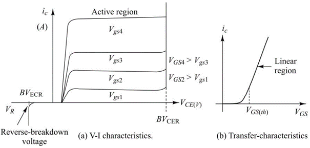
The V-I characteristics of the n-channel IGBT is shown in Figure 14(a). In the forward direction they are like those of the logic level bipolar transistor, the only difference here is that the controlling parameter is the gate-to-source (emitter) voltage (VGS), and the parameter being controlled is the drain (collector) current. When there is no voltage applied to the gate, the IGBT is in the off state. In this state, the current [iD or iC] is zero and the voltage across the IGBT is equal to the source voltage. If a voltage VGS > VGS(th) is applied to the gate, the device turns ON and allows current iD to flow. This current is limited by the source-voltage and the load resistance. In the on-state, the voltage across the IGBT drops to zero.
Figure 14
As shown in Figure 14(a), the drain current (collector current) increases with increase in the gate-to source voltage. Also, VGS is positive. The forward breakdown voltage (BVCER) is the voltage at which the avalanche breakdown takes place. At this point, the voltage across the device and current through it are both high. Hence, the power dissipated in the device will be very large and will damage it. The device must be therefore operated below this voltage.
The transfer characteristic of the IGBT is shown in Figure 14(b). This characteristic is identical to that of the power MOSFET. The characteristic curve is nonlinear for low values of collector current whereas it is linear over most of the range where the collector current is higher. Therefore, in order to operate the IGBT in the linear region of this characteristics, it is necessary to apply VGS greater than VGS(th).


latest video

news via inbox
Nulla turp dis cursus. Integer liberos euismod pretium faucibua