Equalising Network

Equalising Network
Voltage equalisation under these conditions can, however, be achieved by connecting shunt-capacitors as shown in Figure 28. This capacitor removes inequalities in thyristor self-capacitances. Therefore, during turn-off periods, the resultant of self-capacitance and shunt capacitance of each thyristor in a string becomes equal.
Figure 28
During the period for which any of the SCR is in the blocking state, the corresponding capacitor will get charged to the voltage existing across that SCR. When this SCR is turned ON, the capacitor discharges heavy current through this SCR. To limit this discharge current, a damping resistor, RC, is used in series with each capacitor as shown in Figure 28. The value of these damping resistors much be kept to a reasonably low value in order not to reduce the effectiveness of the capacitors in equalising voltage during the reverse recovery interval. Resistor RC also damps out the high-frequency oscillations that may arise due to the ringing of shunt capacitor with circuit inductance. The combination of RC and C is called as the dynamic equalising circuit and is shown in Figure 28.
A diode D is also connected across damping resistor RC. This diode D provides the path for charging the capacitor, when forward voltage appears across the device. Hence, diode D bypasses the resistor RC during charging interval of capacitor C and makes the capacitor more effective in voltage equalisation and for controlling dV/dt across the SCR. In order to prevent ringing, small amount of damping resistance should still be used in series with the diode. While selecting diodes, care must be taken that these diodes must have soft recovery characteristics to avoid high voltage spikes which may be generated due to the abrupt recovery action of diodes.
Equalising Network Design
(1) Static Equalising Network
It is very clear that, a uniform voltage distribution in steady state can be achieved by connecting a suitable resistance across each SCR, such that each parallel combination has the same resistance. This will require different value of resistance for each SCR which is a difficult task. A more practical way of obtaining a reasonably uniform voltage distribution is to connect the same value of resistance R in parallel with each SCR, as shown in Figure 29. This shunt resistance R is called as the static equalising circuit. The value of this shunt resistance can be obtained as follows:
Let ns be the number of thyristors connected in series, as shown in Figure 29. Recall that, in a series string, thyristors with lower leakage current (blocking current) will have to share greater portion of a steady state blocking voltage than will units with higher blocking current. If the range of blocking-current is defined as Ib(max) – Ib(min) = ∆Ib, it is observed that the maximum unbalance in blocking voltage to SCRs of a series string occurs when one member has a blockingcurrent of Ib(min) and all the remaining SCRs have Ib(max). Figure 29 shows such a worst condition.
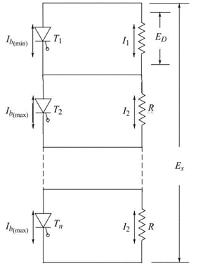
Figure 29
From Figure 29, we can write
$latex \displaystyle {{I}_{{b(\min )}}}+{{I}_{1}}={{I}_{{b(\max )}}}+{{I}_{2}}$
or $latex \displaystyle {{I}_{{b(\max )}}}-{{I}_{{b(\min )}}}={{I}_{1}}-{{I}_{2}}=\Delta {{I}_{b}}$
Let ED be the maximum permissible blocking voltage, then
$latex \displaystyle {{E}_{D}}={{I}_{1}}R$
Now, we can write string voltage ES as $latex \displaystyle {{E}_{S}}={{E}_{D}}+\left( {{{n}_{S}}-1} \right)R\,{{I}_{2}}$
From Equation 1.20, we can write, $latex \displaystyle {{I}_{2}}=\left( {{{I}_{1}}-\Delta {{I}_{b}}} \right)$
Substitute above value of I2 in Equation (1.22)
$latex \displaystyle {{E}_{S}}={{E}_{D}}+\left( {{{n}_{S}}-1} \right)R\left( {{{I}_{1}}-\Delta {{I}_{b}}} \right)$
or $latex \displaystyle {{E}_{S}}={{E}_{D}}+\left( {{{n}_{S}}-1} \right)R\,{{I}_{1}}-\left( {{{n}_{S}}-1} \right)R\,\Delta {{I}_{b}}$
Substitute Equation 1.21 in Equation 1.24
$latex \displaystyle \begin{array}{l}{{E}_{S}}={{E}_{D}}+\left( {{{n}_{S}}-1} \right){{E}_{D}}-\left( {{{n}_{S}}-1} \right)R\,\Delta {{I}_{b}}\\{{E}_{S}}={{n}_{S}}{{E}_{D}}-\left( {{{n}_{S}}-1} \right)R\,\Delta {{I}_{b}}\end{array}$
Now, $latex \displaystyle R\le \frac{{{{n}_{S}}\,{{E}_{D}}-{{E}_{S}}}}{{\left( {{{n}_{S}}-1} \right)\Delta {{I}_{b}}}}$
In general, only the maximum blocking currents for a particular thyristor type are provided by the manufacturer and the ∆Ib value is rarely provided. In such a case, it is usual to assume ∆Ib = Ib(max) with Ib(min) = 0. With this, the value of R calculated from Equation (1.25) is lower than what is actually required. Now, the resistor effective powerdissipation can be expressed as
$latex \displaystyle {{P}_{R}}=\frac{{{{{\left( {{{E}_{{RMS}}}} \right)}}^{2}}}}{R}$
where ERMS is the RMS voltage across R.
(2) Dynamic Equalising Network
As mentioned in the previous section, shunt capacitors are required to limit the rate of rise of voltage on the SCRs and also during the reverse-recovery period, such capacitors provides a reverse recovery current path for slow SCRs around those SCRs which recover first. From Figure 30, it is clear that the maximum unequal distribution of voltage under transient conditions occurs during turn-off due to the difference in the reverse-recovery characteristics. Therefore, the selection of capacitor value C is totally based on the reverse recovery characteristics.
Due to the difference in the reverse-recovery characteristics, the shunt capacitors when charged to peak voltage are not charged equally. Let ns be the number of SCRs connected in series-string, and let us assume that SCR T1 has the fastest recovery and remaining (ns – 1) thyristors have the slowest recovery.
Let ∆Q(max) be the maximum permissible difference between reverse-recovery charge of SCRs of same time and ∆E(max) be the maximum difference in voltage under this situation.
$latex \displaystyle \Delta {{E}_{{\max }}}=\frac{{\Delta {{Q}_{{(\max )}}}}}{C}$
If ED is the maximum permissible blocking voltage of fast SCR (SCR T1), then voltage across remaining (ns – 1) SCRs will be (ED – ∆Emax).
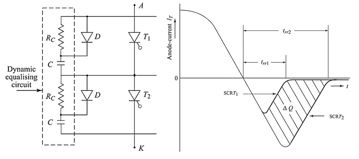
Figure 30
String voltage, $latex {{E}_{S}}={{E}_{D}}+\left( {{{n}_{S}}-1} \right)\left( {{{E}_{D}}-\Delta {{E}_{{\max }}}} \right)$
$latex \,\,\,\,\,\,\,={{E}_{D}}+{{n}_{S}}{{E}_{D}}-{{n}_{S}}\,\Delta {{E}_{{\max }}}-{{E}_{D}}+\Delta {{E}_{{\max }}}$
$latex {{n}_{S}}\Delta {{E}_{{\max }}}-\Delta {{E}_{{\max }}}={{n}_{S}}{{E}_{D}}-{{E}_{S}}$
$latex \Delta {{E}_{{\max }}}\left( {{{n}_{S}}-1} \right)={{n}_{S}}{{E}_{D}}-{{E}_{S}}$
Substituting Equation 1.27 in Equation 1.28, we get
$latex \displaystyle \frac{{\Delta {{Q}_{{(\max )}}}}}{C}\left( {{{n}_{S}}-1} \right)={{n}_{S}}{{E}_{D}}-{{E}_{S}}$
$latex \displaystyle C\ge \frac{{\left( {{{n}_{S}}-1} \right)\Delta {{Q}_{{\max }}}}}{{{{n}_{S}}{{E}_{D}}-{{E}_{S}}}}$
The reverse recovery charge is the function of both the device design characteristics and the circuit commutation conditions. By varying the commutation conditions, such as the magnitude of forward conduction current, circuit inductance and the device junction temperature, the reverse-charge will vary accordingly. The manufacturer specifies the ∆Q for specific conditions.


latest video

news via inbox
Nulla turp dis cursus. Integer liberos euismod pretium faucibua