Dynamic Characteristics of SCR
Dynamic Characteristics of SCR
The static characteristics gives no indication as to the speed at which the SCR is capable of being switched from the forward blocking voltage to the conducting state and vice-versa. However, the transition from one state to the other does not take place instantaneously, it takes a finite period of time.
Dynamic Turn-On Switching Characteristics
This is illustrated in Figure 20. As shown, the total turn-on time ton of the SCR is subdivided into three distinct periods, called the delay time, rise time and spread time. These time periods are defined in terms of the waveforms of the anode voltage and current obtained in a circuit in which the anode-load consists of a pure-resistance.
(i) Delay time (td): This is the time between the instant at which the gatecurrent reaches 90% of its final value and the instant at which the anode current reaches 10% of its final value. It can also be defined as the time during which anode voltage falls from Va to 0.9 Va, where Va is the initial value of the anode voltage. The gate current has non-uniform distribution of current density over the cathode surface due to the p-layer. Its value is much higher near the gate but decreases rapidly as the distance from the gate increases. It shows that during td, anode current flows in a narrow region near the gate where gate current density is the highest.
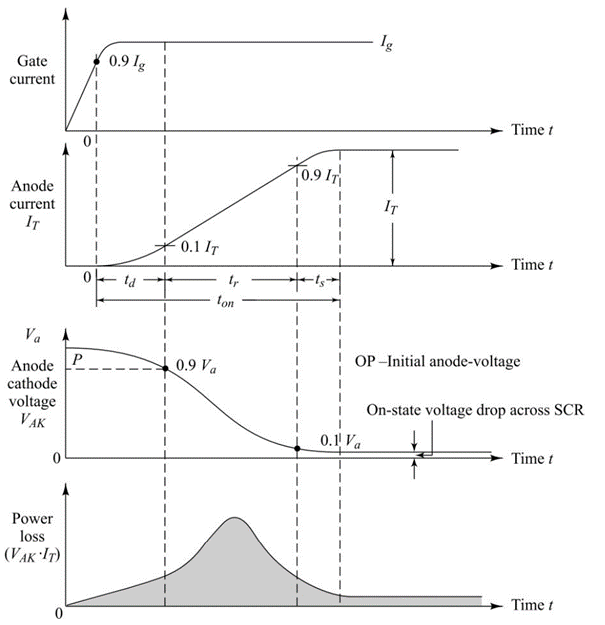
Figure 20
(ii) Rise Time (tr): This is the time required for the anode current to rise from 10 to 90% of its final value. It can also be defined as the time required for the forward blocking off-state voltage to fall from 0.9 to 0.1 of its initial value-OP. This time is inversely proportional to the magnitude of gate current and its build up rate. Thus, tr can be minimized if high and steep current pulses are applied to the gate. For series RL circuit, the rate of rise of anode current is slow, therefore, tr is more and for the RC series circuit, di/dt is high thus tr is less. During rise-time, turn-on losses are the highest due to high anode voltage Va and large anode current IT occurring together in the thyristor.
(iii) Spread-time (ts): The spread time is the time required for the forward blocking voltage to fall from 0.1 to its value to the on-state voltage drop (1 to 1.5 V). After the spread time, the anode current attains steady-state values and the voltage drop across SCR is equal to the on-state voltage drop of the order of 1 to 1.5 V.
(iv) Turn-on Time (ton): This is the sum of the delay time, rise time and spread time. This is typical of the order of 1 to 4 ms, depending upon the anode circuit parameters and the gate signal waveshapes.
The width of the firing pulse should, therefore, be more than 10 ms, preferably in the range of 20 to 100 ms. The amplitude of the gate pulse should be 3 to 5 times the minimum gate current required to trigger the SCR.
From Figure 20, it is noted that during rise-time, the SCR carries a large forward current and supports an appreciable forward voltage. This may result in high instantaneous power dissipation creating local internal hot spots which could destroy the device. It is, therefore, necessary to limit the rate of rise of the current. Normally, a small inductor, called di/dt inductor is inserted in the anode circuit to limit the di/dt of the anode current.
The shadow area under the power curve in Figure 20 represents the switching loss of the device. This loss may be significant in high-frequency applications.
Dynamic Turn-Off Switching Characteristics
Once the SCR starts conducting an appreciable forward current, the gate has no control over it and the device can be brought back to the blocking state only by reducing the forward current to a level below that of the holding current. The process of a turn-off is also called commutation. However, if a forward voltage is applied immediately after reducing the anode current to zero, it will not block the forward voltage and will start conducting again, although it is not triggered by a gate pulse. It is, therefore, necessary to keep the device reverse biased for a finite period before a forward anode voltage can be reapplied.
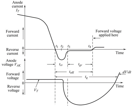
The turn-off time of the thyristor is defined as the minimum time interval between the instant at which the anode current becomes zero, and the instant at which the device can block the forward voltage. The turnoff time is illustrated by the waveforms shown in Figure 21. The total turn-off time toff is divided into two time-intervals the reverse recovery time trr and the gate recovery time tgr.
At the instant t1, the anode forward current becomes zero. During the reverse recovery time, t1 to t3, the anode current flows in the reverse direction. At the instant t2, a reverse anode voltage is developed, and the reverse recovery current continues to decrease. At t3, junctions J1 and J3 can block a reverse voltage. However, the thyristor is not yet able to block a forward voltage because carriers, called trapped charges, are still present at junction J2. During the interval t3 to t4, these carriers recombine. At t4, the recombination is complete and therefore, a forward voltage can be reapplied at this instant. The SCR turn-off time is the interval between t4 and t1. In an SCR, this time varies in the range 10 to 100 ms. Thus, the total turn-off time (tq) required for the device is the sum of the duration for which the reverse recovery current flows after the application of reverse voltage, and the time required for the recombination of all excess carriers in the inner two layers of the device. This may be noted that in a highly inductive load circuit, the current cannot change abruptly at t1. Also, the fast change in current at t2 may give rise to high voltage surges in the inductance, which will then appear across the terminals of the thyristor.
Figure 21
In practical applications, the turn-off time required to the SCR by the circuit called the circuit turn-off time tq, must be greater than the device turn-off time toff by a suitably safe margin, otherwise, the device will turn on at an undesired instant a process known as commutation failure. Thyristor having large turn-off time (50 – 100 ms) are called slow switching or phase control type thyristors (or converter grade thyristors), and those having low turn-off time (10 – 50 ms) are called fast switching or inverter type thyristors. In high-frequency applications, the required circuit turn-off time consumes an appreciable portion of the total cycle time and therefore, inverter-grade thyristors must be used.


latest video

news via inbox
Nulla turp dis cursus. Integer liberos euismod pretium faucibua