Structure and Working of Solar Cells

A p-type semiconductor is formed when an intrinsic semiconductor is doped with an electron-accepting element. For example, aluminum (Al) has three valence electrons which when doped with silicon form three covalent bonds, and one hole or electron vacancy is created.
An n-type semiconductor is formed when an intrinsic semiconductor is doped with an electron donor element. For example, Phosphorus (P) has five valence electrons which when doped with silicon form four covalent bonds, with one electron is free.
The basic cell structure of a typical N-on-P, bulk silicon cell is shown in Fig. 1.1. The bulk material is P-type silicon with thickness 100 to 350 microns, depending on the technology used. A thin layer of N-type silicon is formed at the top surface by diffusing an impurity from Vth group (phosphorus being most common) to get a PN junction. The top active surface of the N layer has an ohmic contact with metallic grid structure to collect the current produced by impinging photons. The metallic grid covers minimum possible top surface area (less than 10 per cent of the total area) to leave enough uncovered surface area for incoming photons. Similarly, the bottom inactive surface has an ohmic metallic contact over the entire area. These two metallic contacts on P and N layers respectively form the positive and negative terminals of the solar cell. In addition to basic elements, several enhancement features are also included in the construction. For example, providing antireflective coating, textured finish of the top surface and reflective, textured rear surface, to capture maximum photons and direct them toward the junction.
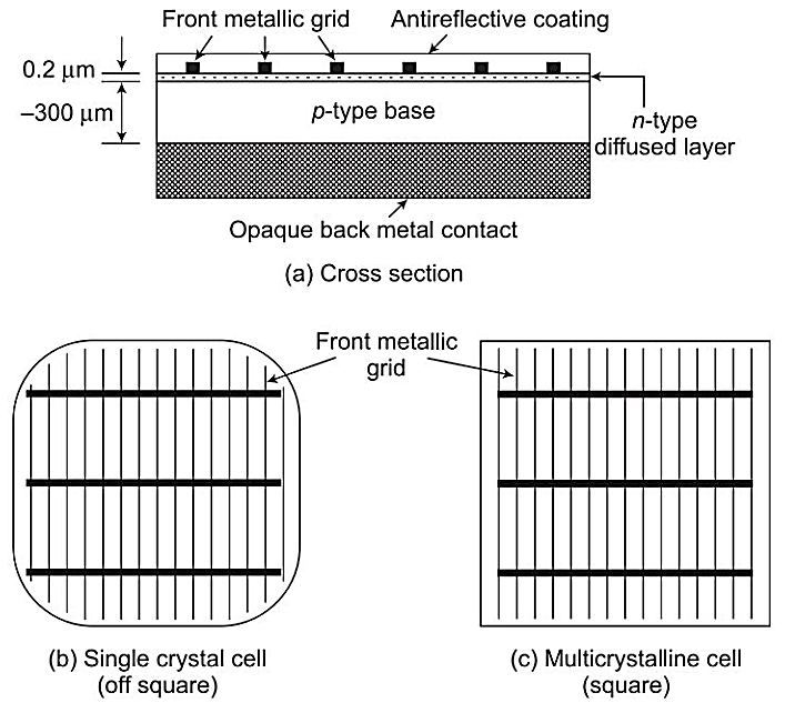
Fig. 1.1: Construction of Solar Cell
A PN junction, where the material changes suddenly from P to N is known as abrupt PN junction. An abrupt junction is an idealization because the P side cannot suddenly end where the N side begins. In a more realistic PN junction there is a gradual change from one type of material to another. Such a junction is known as graded junction.
When a junction between a P-and N-type materials is formed, the carriers (free electrons and holes) diffuse from higher concentration side to lower concentration side. Soon after crossing the junction, these carriers recombine with the other types of carriers found in majority on the other side. We see that the holes, which neutralized the acceptor ions near the junction in the P-type side, disappeared because of recombination with free electrons, which have diffused from across the junction. Similarly, free electrons near the junction in the N-type side have recombined with holes, which have crossed the junction from P side. The un-neutralized ions in the neighbourhood of the junction result in a charge density. Since this region is depleted of mobile charges it is called depletion region, the space charge region or transition region. The charge distribution, which is zero at the junction, constitutes an electric dipole; that is, it is positive on one side and negative on the other side. This electrostatic potential variation causes an electric field in the depletion region, which points from positive to negative charge, i.e., N side to P side. This voltage variation constitutes a potential energy barrier against further diffusion of free electrons and holes to the other side of the junction. This is known as contact potential, barrier voltage VB or potential energy hill (due to its shape). Figure 1.2 shows charge density, electric field intensity, and barrier voltage for free electrons. The shapes of the curves depend on how a junction is graded and the doping level.
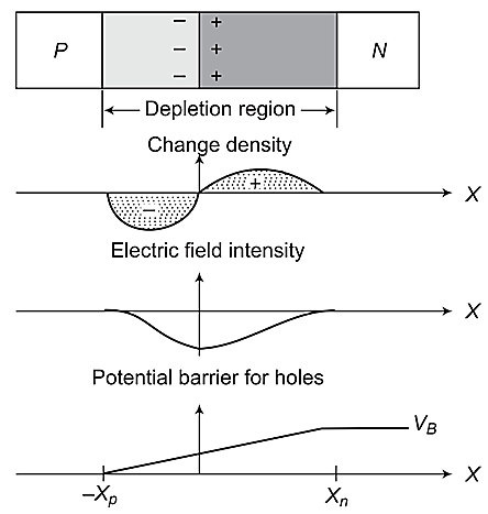
Fig. 1.2: Charge density, electric field intensity and potential barrier in a PN junction
The energy available in a photon is given by:
![]()
![]() (1)
(1)
where h is Planck’s constant (h = 6.63×10⁻³⁴ joules-sec), c is the speed of light, v is frequency of photons and λ is the wavelength of photons.
The energy in a photon must exceed the semiconductor band gap energy, EG to get absorbed and generate an electron-hole pair. For energies less than band gap energy, no absorption takes place. The material appears transparent to these low energy photons. If a photon has energy much greater than the band gap, it still produces a single electron-hole pair. The remainder of photon energy is lost to the material as heat. Therefore, it is desirable that the semiconductors used for photo absorption have band gap energy such that maximum percentage of solar spectrum is efficiently absorbed. For silicon, which has band gap of 1.12 eV, photons of λ = 1.1 μm or less are required to produce electron-hole pair.
Once an electron-hole pair is generated within the depletion region, both carriers will be acted upon by the built in electric field. Since the field is directed from N to P side, it will cause the holes to be swept quickly towards the P side and the electrons to be swept quickly towards the N side. Due to the electric field, chances of recombination of these electron-hole pairs are quite less. Once out of depletion region, these carriers become a part of the majority carriers in the respective regions and diffuse away from the depletion region as their concentration near junction has increased. Addition of excess majority charge carriers on each side of the depletion region results in a voltage across external terminals of the junction. If a load is connected across these terminals, the photon-generated current will flow through this external circuit. This current will be proportional to number of electron hole pairs generated, which in turn depends on intensity of illumination. Thus, an illuminated PN junction becomes a photovoltaic cell with positive terminal on P side.
Now, consider the case when an electron-hole pair is generated outside the depletion region (i.e. in quasi-neutral region) then, depending on, how far it is located from the depletion region, it may or may not contribute to photocurrent.


latest video

news via inbox
Nulla turp dis cursus. Integer liberos euismod pretium faucibua