Classification of Solar Cells
Classification of Solar Cells
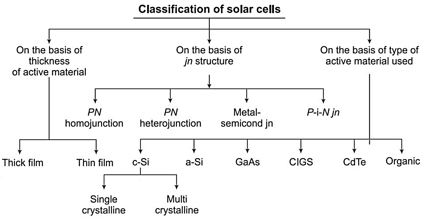
Solar cells may be classified based on (i) thickness of active material, (ii) type of junction structure, and (iii) the type of active material used in its fabrication, as shown in the chart below.
Apart from this, solar cells are also divided into three main categories called generations. The first generation include wafer-based mono and multi-crystalline solar cells. At present, solar cells of first generating are dominating the market. The second-generation solar cells include thin film cells such as amorphous silicon, CIGS and Cadmium Telluride, etc. These solar cells are available commercially. The third-generation solar cells operate on entirely different principle. They include dye sensitized, organic and quantum dot solar cells, etc. The third-generation solar cells are under development stage.
On the Basis of Thickness of Active Material: Depending on the thickness of the active material, they are classified as: (i) thick film cell and (ii) thin film cell. In thick film cells, base material (starting material in fabrication process) itself is an active material. In thin film cells, a thin film (few nm to 10s of μm) deposition of active material is carried out on the back support sheet, known as a substrate. Thin film solar cells have the major advantage of significantly low, active material consumption and the possibility of continuous sequence of production processes.
On the Basis of Junction Structure: On the basis of the type of junction structure they are classified as (i) PN homojunction cell and (ii) PN heterojunction cell, (iii) PN multijunction cell, (iv) metal-semiconductor (Schottky) junction and (v) P-i-N (P-type-intrinsic-N-type) semiconductor junction.
In homogeneous PN junction, the semiconductor material on both sides of the junction is same, only doping materials are different. Thus, the band gap remains same throughout the cell material. Most of the electron hole pairs generated in the top layer are lost to recombination when they are created more than a diffusion length from the junction.
On the other hand, in heterogeneous PN junction, two dissimilar semiconductor materials, such as group III-V or group II-VI compound semiconductors with closely matching crystal lattice are used to form the junction. The band gap of the top material, exposed to sunlight is wider than the band gap of the material below the junction. As a result, the higher band gap region will appear transparent to photons with lower energies, so they can penetrate to the junction where the band gap is less than the incident photon energy. Thus electron-hole pairs are generated within or near depletion region, where they are collected before they recombine.
When a contact is made between a metal and semiconductor, either an ohmic contact or a rectifying contact is formed depending on the work functions of metal and semiconductor. The rectifying contact is known as Schottky junction. The Schottky barrier junction is relatively straightforward to fabricate but is not very efficient as a PV cell since it has relatively smaller open circuit voltage than conventional PN junction.
Solar spectrum has photons of varying energies (from UV to IR region). A photon is most efficiently absorbed when its energy is close to band gap. A clever way to absorb more photon energy is to stack junctions of different band gaps, what is known as multijunction structure. The top junction has a relatively wider band gap followed by one or two more junctions in decreasing order of band gaps, in tandem (series). High-energy photons will be absorbed at the top junction followed by absorption of lower energy photons at subsequent junctions. This P-i-N structure is used in amorphous-silicon solar cells.
On the Basis of Type of Active Material: Depending on the type of material used for fabrication of a junction, they are classified as: (i) single crystal (or monocrystalline) silicon cell, (ii) multi-crystalline silicon cell, (iii) amorphous silicon (a-Si), (iv) gallium arsenide cell (GaAS), (v) copper indium (gallium) di-selenide cell (CIS), (vi) cadmium telluride cell (CdTe) and (vii) organic PV cell. At present, only single crystal, multi-crystalline and to some extent CIS, CdTe and a-Si cells are being produced commercially.
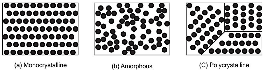
Fig. 1.8: Atomic arrangement of mono, amorphous and polysilicon
In single crystal or mono crystalline silicon there is a perfect periodic arrangement of atoms. The crystal is highly ordered, and its lattice is continuous and unbroken. Amorphous Si is non-crystalline, and its atoms do not display any structures and they are not arranged in an ordered manner. Polycrystalline (and multi-crystalline) Si structure is in between these two extremes. These materials are composed of many crystallites of varying size and orientation. Crystallites are also referred to as grains as shown in Fig. 1.8.


latest video

news via inbox
Nulla turp dis cursus. Integer liberos euismod pretium faucibua